- table of contents
2F
You can check the corresponding device by clicking the number in the image.
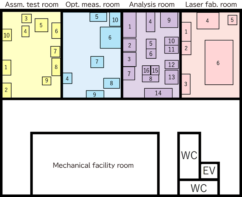
Assembly test room
- 1 UV exposure
- 2 Palylene evaporator
- 3 Flip chip bonder#2(M-90-10)
- 4 Wire bonder#1(L026-343)
- 5 Dicer
- 6 Fume hood
- 7 Spin Coater
- 8 Fume hood
- 9 Electroplating #1(2401), #2(HAB-151A)
- 10 Wire bonder#2(HB16)
Optical measurement room
Analysis room
- 1 SEM
- 2 FIB
- 3 Ultraviolet spectroscopic ellipsometer(M-2000D-Tm)
- 4 Ion coater
- 5 SEM sample Polisher
- 6 SEM sample Ion milling
- 7 TG/DTA
- 8 UV/Vis/IR spectrometer
- 9 XRD#2(D8 ADVANCE)
- 10 Microsystem Analyzer(MSA-500)
- 11 Microsystem Analyzer(MSA-400)
- 12 High-frequency laser doppler vibrometer
- 13 Thin film characterization system
- 14 FT-IR
- 15 3D Laser Scanning Microscope(VK-X3000/X3050)
- 16 AFM(Nano Wizard NSK)
Laser fabrication room
- 1 YAG Laser
- 2 VIM, Fluorescence microscope
- 3 Fume hood
- 4 PLD
- 5 Hall effect measurement
- 6 MBE