Smart System Super Integration Research Center, Tohoku University
HOMEFacilitiesShape/morphology observation, analysis
FacilitiesShape/morphology observation, analysis
- table of contents
Shape/morphology observation, analysis
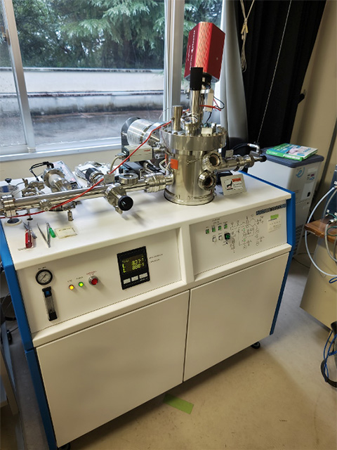
Thermal Decomposition Spectroscopy
| Manufacturer name (model) | ESCO (WA1000) |
| Use | Temperature rise desorption gas analysis on silicon or glass substrates |
| pplication example | Amount of H2O adsorbed on SiO2 and desorption temperature analysis, Amount of H+ adsorbed on Si and desorption temperature analysis |
| Sample size | 1 × 1 cm |
| Others | No organic materials accepted, no organically contaminated samples accepted |
| Remarks | Contamination control is required. Consult with the person in charge of equipment management (Shuji Tanaka Laboratory) before use. |
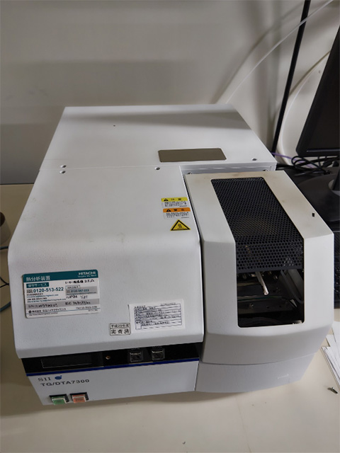
TG/DTA
| Manufacturer name (model) | SII (TG/DTA7300) |
| Sample size | Maximum sample volume 200mg or the amount that can be contained in the container |
| Others | Measuring temperature range: RT to 1500℃, TG measuring range: ±400 mg, TG sensitivity: 0.2 μg, DTA measuring range: ±1000 μV, DTA sensitivity: 0.06 μV |
| Remarks | |
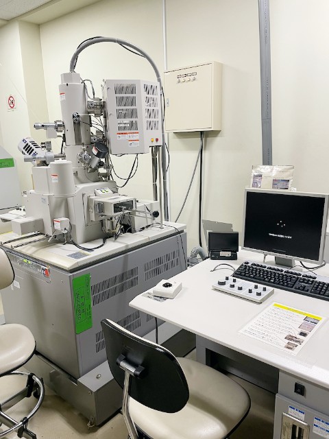
SEM
| Manufacturer name (model) | SEM: Hitachi High-Tech (SU-70), EDX: Oxford (AZtec Energy X-Max)
|
| Application | Observation of fine structure of sample
|
| Sample size | Maximum ⌀6 inch
|
| Application example | Observation of fine shape on the order of nm, element analysis by EDX
|
| Main specifications | Electron gun: ZrO/W Shotkey emission type electron gun, acceleration voltage: 0.5–30 kV
|
| Remarks | |
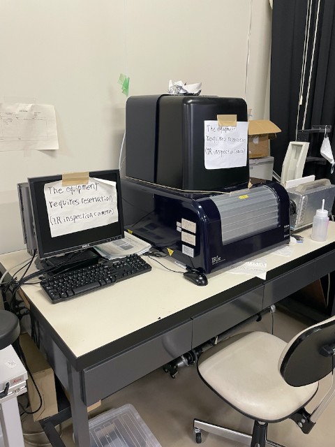
IR inspection camera
| Manufacturer name (model)) | Moritex (IRise) |
| Use | Internal inspection of sample |
| Sample size | Maximum ⌀8 inch |
| Application example | Evaluation of joint interface of joint sample |
| Evaluation of joint interface of joint sample | Monitor magnification: 33–1760 times |
| Other | The entire wafer can be evaluated collectively by combining images.
|
| Remarks | |
ESCA
| Manufacturer name (model) | ULVAC PHI (ESCA1600)
|
| Use | Element analysis of sample surface |
| Sample size | Maximum ⌀2 inch |
| Application example | Sample surface composition analysis, chemical bond state evaluation
|
| Main specifications | X-ray source: Mg, Al (not monochrome)
|
| Others | Depth direction analysis possible by Ar etching, Auger electron spectroscopy Measurement |
| Remarks | |
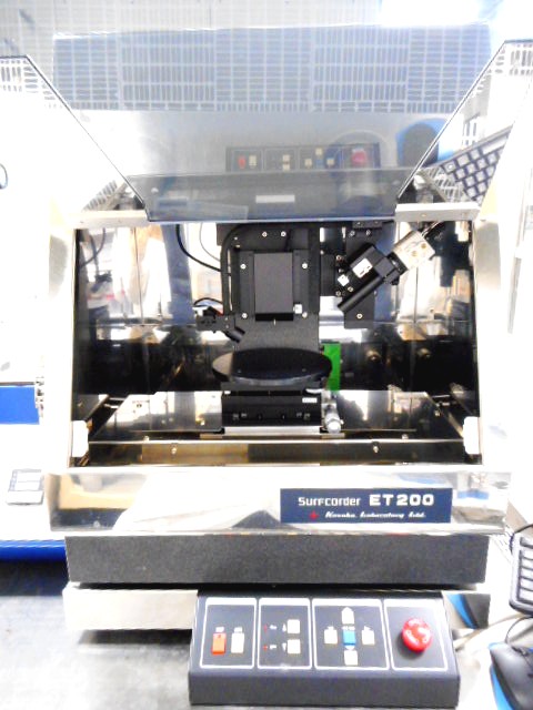
Surface profilometer
| Manufacturer name (model) | Kosaka Laboratory (ET200) |
| Application | Sample surface shape measurement (line analysis)
|
| Sample size | ⌀160 mm × Thickness 48 mm
|
| Application example | Si after etching Wafer shape measurement |
| Main specifications | Height resolution: 0.1 nm, Lateral resolution: 0.1 μm
|
| Remarks | |
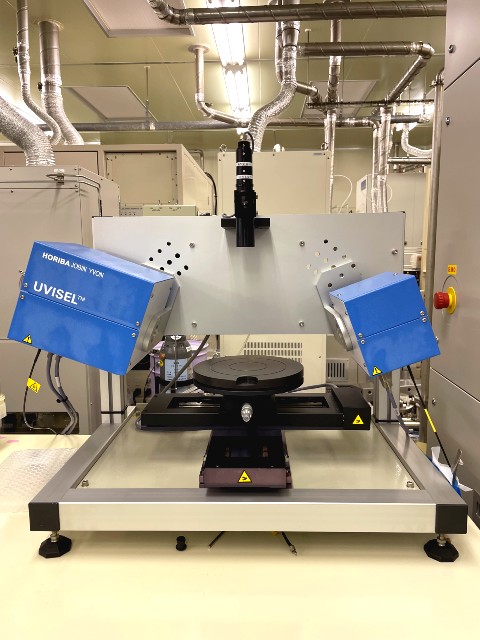
Ellipsometer(UVISEL)
| Manufacturer name (model) | HORIBA JOBIN YVON (UVISEL-LT)
|
| Use | Film thickness analysis, optical constants (n, k) analysis, in-plane distribution measurement
|
| Sample size | Maximum ⌀8 inch
|
| Application example | Measuring the film thickness and refractive index of the |
| Main specifications | Wavelength: 260–2100 nm, [Light source] Xe lamp (75 W)
|
| Other | Supports wavelengths from ultraviolet to near infrared. Automatic in-plane distribution measurement with an electric stage.
|
| Remarks | |
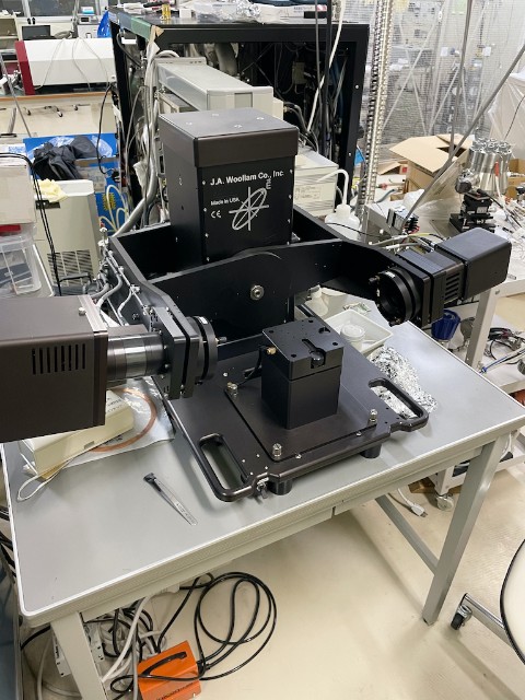
Ultraviolet spectroscopic ellipsometer(M-2000D-Tm)
| Manufacturer name (model) | J.A. Woollam (M-2000D)
|
| Use | Measurement of thin film thickness and optical constant |
| Sample size | Maximum □5 inch |
| Application example | Measurement of film thickness of |
| Main specifications | Measurement wavelength range: 193–1000 nm |
| Remarks | |
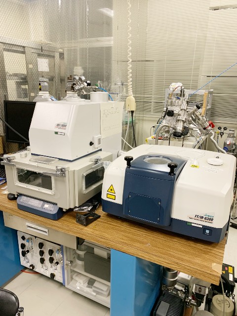
FT-IR
| Manufacturer name (model) | Japan Spectroscopy (main unit: FT / IR-6300, microscopic part: IRT-7000)
|
| Application | Infrared spectroscopic measurement of sample |
| Sample size | ⌀4 inch (depending on the measurement method)
|
| Application example | Film quality analysis of thin film
|
| Main specifications | Transmission, reflection, ATR, RAS, measurement in vacuum state, microscopic measurement possible
|
| Remarks | |
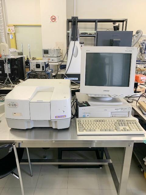
UV/Vis/IR spectrometer
| Manufacturer name (model) | Jasco (V-570) |
| Use | Measurement of sample absorbance |
| Sample size | Maximum ⌀2 inch
|
| Application example | Measurement of absorbance of thin film |
| Main Specifications | Measurement wavelength range: 190–2500 nm, target sample: solid, liquid, measurement method: transmission measurement, reflection measurement
|
| Remarks | |
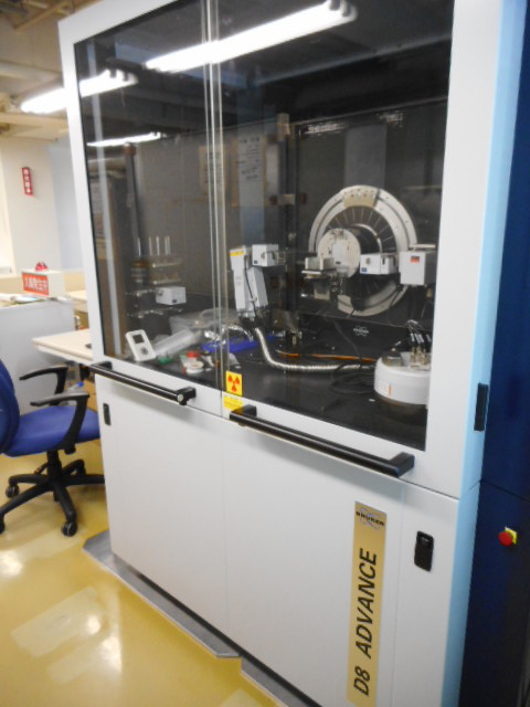
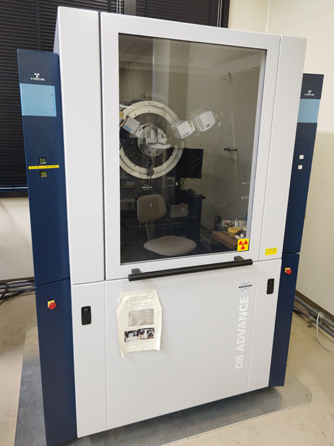
XRD#1(D8 ADVANCE)
| Manufacturer name (model) | Bruker (D8 ADVANCE) |
| Application | Sample crystal structure evaluation, θ/2θ measurement, Rocking curve measurement, pole diagram measurement, residual stress measurement, etc. |
| Sample size | Maximum ⌀2 inch |
| Main specifications | Two-dimensional X-ray diffraction pattern can be acquired by a two-dimensional detector.
|
| Remarks | |
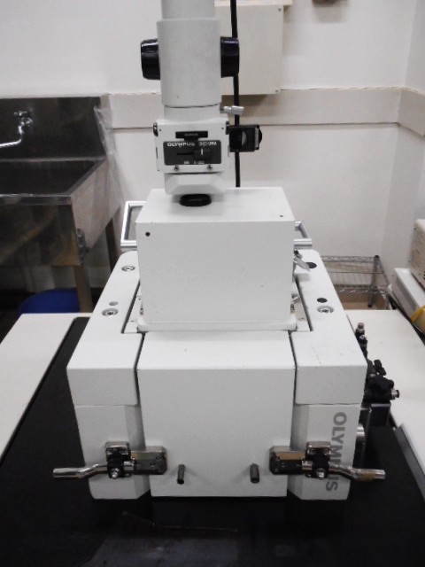
Olympus SPM
| Manufacturer name (model) | Olympus (NV-2000)
|
| Application | Acquisition of surface shape image and conductive image of minute area
|
| Sample size | ⌀20 mm or less is recommended
|
| Application example | Observation of the metal film surface. |
| Others | Data is retrieved using an MO drive, and files are also in a special format.
|
| Remarks | |
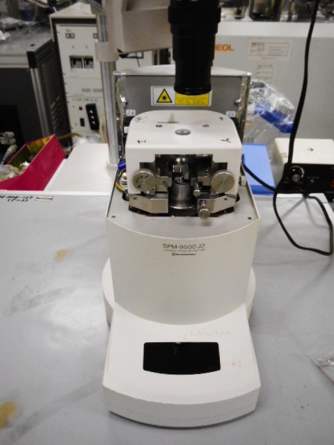
SPM (Shimazu, 9500J2)
| Manufacturer name (model) | Shimadzu Corporation (SPM9500-J2) |
| Use (features) | Acquisition of surface shape images and conductive images of minute regions
|
| Sample size | Within ⌀15 mm |
| Application example | Observation of the metal film surface. |
| Others | The operation is unstable because the control board is out of order and cannot be repaired. |
| Remarks | |
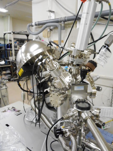
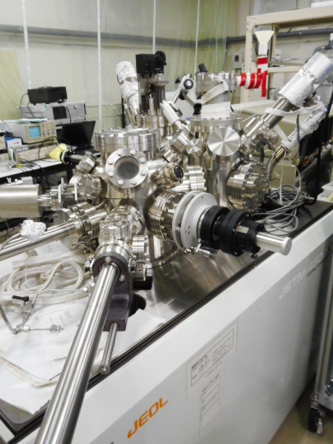
UHV-STM & AFM
| Manufacturer name (model) | JEOL (JSTM-4500XT) |
| Application | Surface shape measurement |
| Sample size | About 2 × 5mm |
| Application example | Measurement with atomic resolution (STM) |
| Others | The operation of the device requires considerable knowledge and training. |
| Remarks | |
XRD#2(D8 ADVANCE)
| Manufacturer name (model) | Bruker (D8 ADVANCE) |
| Purpose | Evaluation of sample crystal structure, θ/2θ measurement |
| Maximum Rated Output | 3kW (Maximum tube voltage, tube current: 60kV – 60mA) |
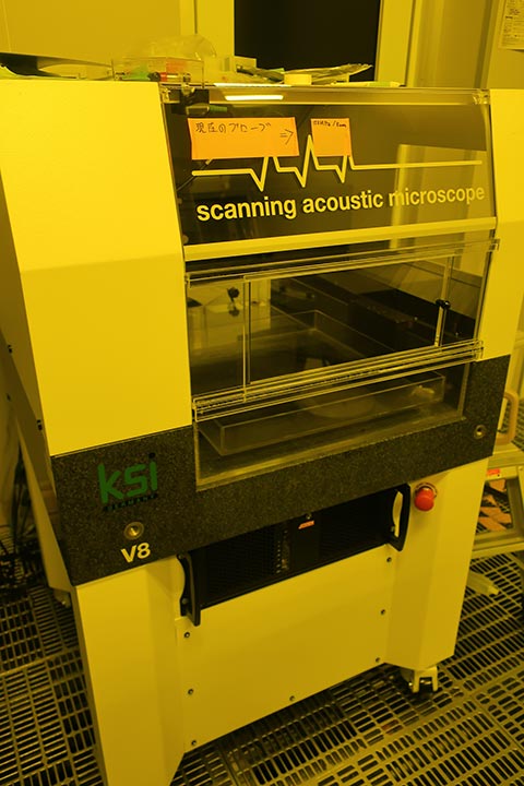
Scanning acoustic microscope (KSI)
| Manufacturer name (model) | KSI(V-8A) |
| Application | Bonding interface observation |
| Main specifications | soak in water |
| Sample size | Within 12inch square |
| Others | |
| Remarks | |
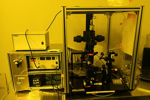
Contact angle meter(Kyowa)
| Manufacturer name (model) | Kyowa(MCA-3/J) |
| Application | Contact angle measurement |
| Main specifications | High-speed camera
Frame rate: 60fps |
| Sample size | Within 20mm square |
| Others | |
| Remarks | |
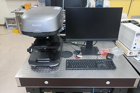
3D Laser Scanning Microscope(VK-X3000/X3050)
| Manufacturer name (model) | Keyence – VK-X3000 |
| Application | 3D surface observation |
| Sample size | 4inch |
| Others | 3D observation, thin film thickness, roughness measurement |
| Remarks | |
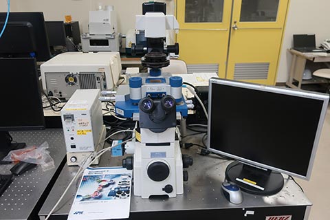
AFM(Nano Wizard NSK)
| Manufacturer name (model) | JPK instrument(Nano Wizard NSK) |
| Application | Surface observation |
| Main specifications | Contact mode, intermittent mode, phase correction |
| Sample size | 4inch |
| Others | Conductive needle available |
| Remarks | |
Contact angle meter(DMe201)
| Manufacturer name (model) | Kyowa – DMe201 |
| Application | Contact angle measurement |
| Sample size | 4inch |
| Others | Surface tension |
| Remarks | |
Microscope(KH-7700)
| Manufacturer name (model) | HiROX KH-7700 |
| Application | Surface observation |
| Sample size | 4inch |
| Others | |
| Remarks | |
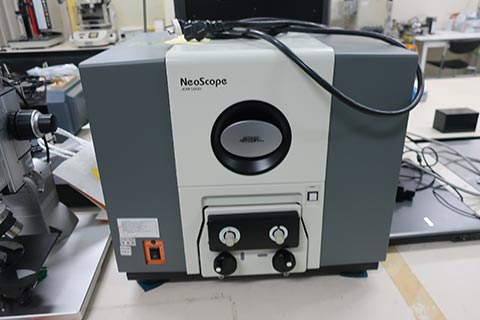
Table top SEM(JCM-500)
| Manufacturer name (model) | JEOL Neoscope-N JCM-500 |
| Application | Surface observation |
| Sample size | 4inch |
| Others | |
| Remarks | |
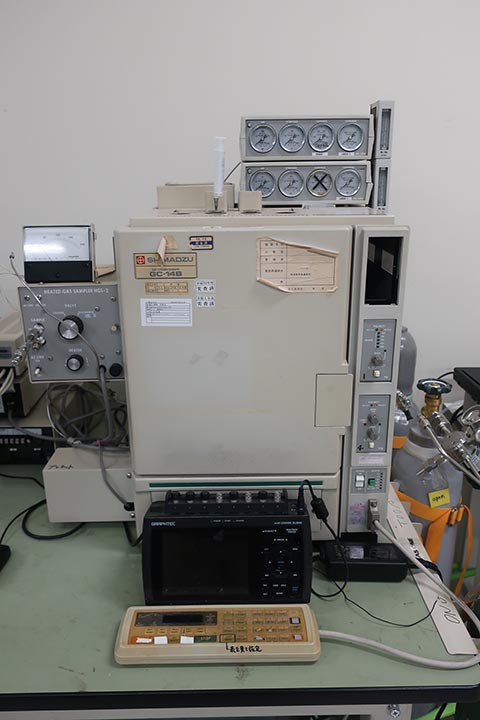
Gas Chromatograph#1(GC-14B)
| Manufacturer name (model) | SHIMADZU(GC-14B) |
| Others | |
| Remarks | |
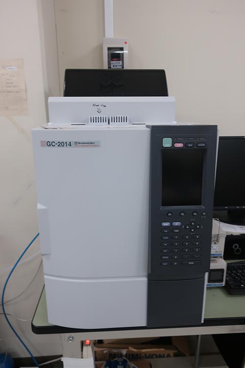
Gas Chromatograph#2(GC-2014AF)
| Manufacturer name (model) | SHIMADZU(GC-2014AF) |
| Others | |
| Remarks | |