Request for Acknowledgments
Please include an acknowledgment to the Smart System Super Integration Research Center (SIRC), Tohoku University, when publishing research outcomes obtained through the use of SIRC facilities, equipment, or support.
The wording may be adjusted as appropriate depending on the nature of the support provided.
Sample Acknowledgments
- (Part of) this study was performed at the Smart System Super Integration Research Center (SIRC), Tohoku University.
- This study used facilities/equipment at the Smart System Super Integration Research Center (SIRC), Tohoku University.
Three-dimensional imaging of electron spin resonance-magnetic resonance force microscopy at room temperature
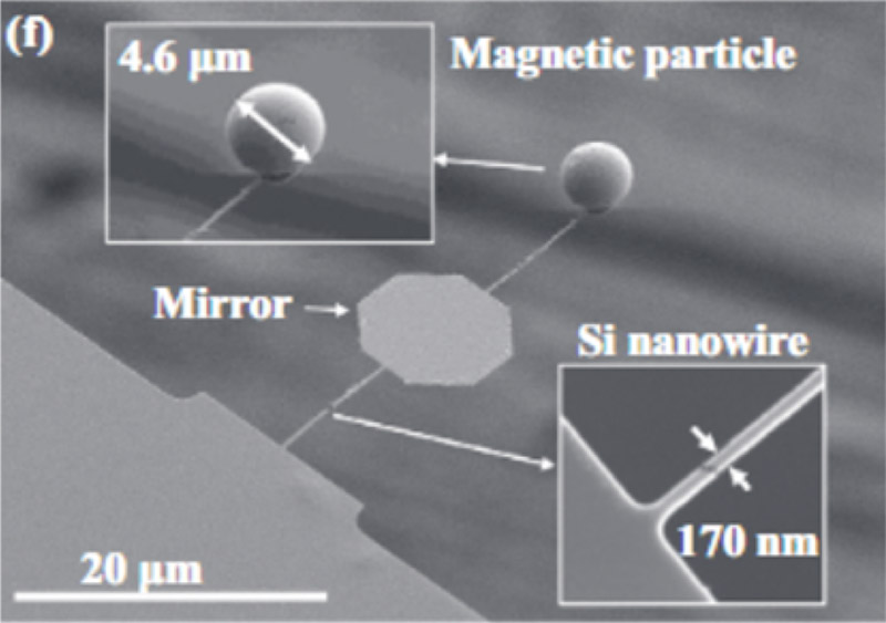
The three-dimensional (3D) imaging by magnetic resonance force micro-scopy (MRFM) based on electron spin resonance (ESR) measurement is demonstrated at room temperature. For a microsample containing radicals, the 3D force distribution was obtained using a custom-made Si nano-wire and a permanent magnet. This result contributes to improving the long scanning time and achieving the high sensitive and wide range measurement.
| Used equipment | EB lithography system, FAB, mask aligner (SUSS), ICP-RIE #2 |
|---|---|
| Article | Masaya Toda and Takahito Ono, “Three-dimensional imaging of electron spin resonance-magnetic resonance force microscopy at room temperature,” Journal of Magnetic Resonance 330, 107045 (2021). https://doi.org/10.1016/j.jmr.2021.107045 |
Evaluation of Microfluidic Channels With Thin Si Windows and Trapping Structures
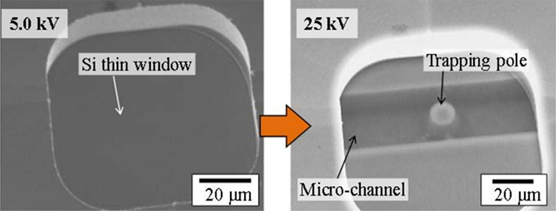
The fabrication and evaluation of a microchannel with thin Si windows and a trapping structure for injected liquid samples is demonstrated. East cells and latex particles were observed using a scanning electron microscope (SEM) under vacuum.
| Used equipment | Mask aligner (SUSS), CCP-RIE #1, RF magnetron sputter (Shibaura) #2, electroplating, ion beam milling, ICP-RIE #2, thermal electron SEM |
|---|---|
| Articlle | Masaya Toda, Hideki Hayashi, Nguyen van Toan, Naoki Inomata, and Takahito Ono, “Evaluation of Microfluidic Channels With Thin Si Windows and Trapping Structures,” Journal of Microelectromechanical Systems 30(4), 560–568 (2021). https://ieeexplore.ieee.org/document/9431372 |
Vertically-oriented graphene electrodeposited with MnO2 on native SiO2/Si for high-performance supercapacitor electrodes
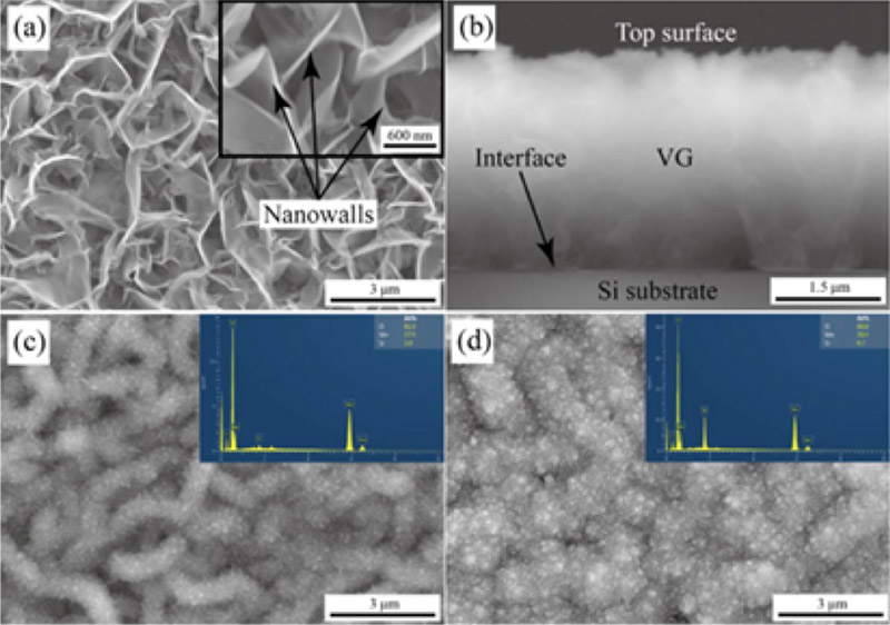
Supercapacitor electrodes, composed of vertically-oriented graphene (VG) and MnO2, are synthesized on native SiO2-passivated silicon wafers. The VG layers with a thickness of ~3 μm are deposited directly on the substrates. The specific capacitance as high as 470.80 mF/cm2 at 20 mV/s is achieved with the increasing loadings of MnO2. The original retention of 99.29% after 5000 cycles demonstrates the excellent cycling stability, which is ascribed to the strong bonds between VG/SiO2/Si and MnO2/VG.
| Used equipment | Plasma diamond CVD |
|---|---|
| Article | Hongtao Sui, Nguyen Van Toan, and Takahito Ono, “Vertically-oriented graphene electrodeposited with MnO2 on native SiO2/Si for high-performance supercapacitor electrodes,” Journal of Electroanalytical Chemistry 895, 115507 (2021). https://doi.org/10.1016/j.jelechem.2021.115507 |
A magnetic actuator with parylene spring
An actuator with large displacement is beneficial for camera shake compensation, but conventional MEMS electrostatic actuators are unable to achieve a displacement more than hundreds of µm. We, therefore, developed a magnetic actuator with a large displacement of 200 µm using soft springs of parylene and magnets embed in a Si substrate.
| Used equipment | Sputtering machine, parylene coater, ICP-RIE #3 |
|---|---|
| Article | Huayu Wang, Masashi Matsuura, Shusuke Yamada, Satoshi Sugimoto and Shuji Tanaka, “Temperature stable rare earth magnetic powder Sm-Fe-N based micro magnets with remanence enhanced by easy axis alignment and its application in MEMS actuator,” J. Micromech. Microeng. (2021) 075002 (10pp), May. 2021, pp. 1–10. https://doi.org/10.1088/1361-6439/abfeb3 |
Terahertz tunable filters using MEMS metamaterials
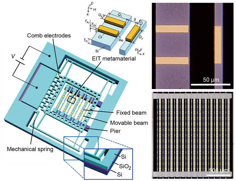
By moving the components of metamaterials by microactuators, it is possible to realize a “MEMS metamaterials” that has both the unique optical characteristics of the metamaterials and dynamic tunability. We have developed a transmittance tunable filter by incorporating a microactuator into an electromagnetically induced transparency (EIT) metamaterial that responds in the terahertz band and controlling the gap between the dipoles and quadrupoles that makes up the EIT metamaterial. It is expected to be applied to terahertz wave control, which plays an important role for next-generation wireless communication (Beyond 5G/6G).
| Used equipment | Laser lithography system, mask aligner (SUSS), RF magnetron sputter (Shibaura), ICP-RIE |
|---|---|
| Article | Y. Huang, K. Nakamura, Y. Takida, H. Minamide, K. Hane, and Y. Kanamori, “Actively tunable THz filter based on an electromagnetically induced transparency analog hybridized with a MEMS metamaterial,” Scientific Reports 10, 20807 (2020). https://doi.org/10.1038/s41598-020-77922-1 |
Optical force sensors using movable metamaterials
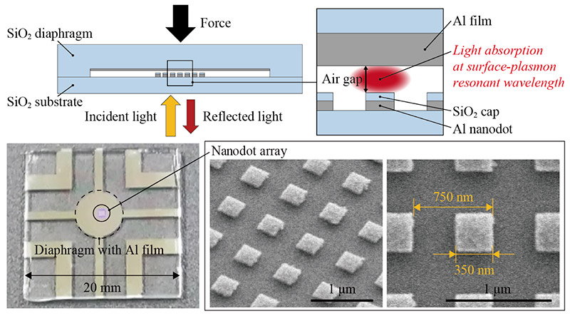
If the dielectric layer that constitutes metal-dielectric-metal (MIM) metamaterials is an air gap, it is possible to construct “movable metamaterials” in which the thickness of the dielectric layer changes due to force. We have developed an optical force sensor that can measure the force applied on the diaphragm by measuring the resonance peak shift seen in the reflection spectrum. This sensor can achieve higher sensitivity than the conventional Fabry–Pérot interferometric optical force sensor.
| Used equipment | EB lithography system, EB evaporator, ion beam milling, high resolution SEM |
|---|---|
| Article | T. Okatani, S. Sekiguchi, K. Hane, and Y. Kanamori, “Surface-plasmon-coupled optical force sensors based on metal–insulator–metal metamaterials with movable air gap,” Scientific Reports 10, 14807 (2020). https://doi.org/10.1038/s41598-020-71825-x |
Development of Large Integrated Flexible Hybrid Electronics with Advanced Semiconductor Packaging
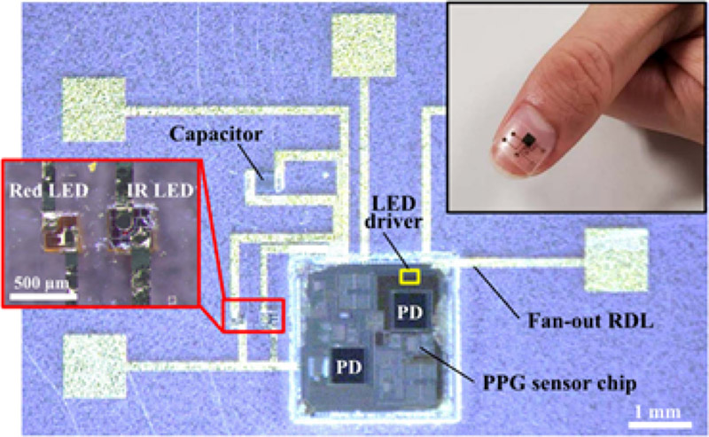
In order to improve the performance, integration, and flexibility of flexible devices, we have conducted research on hetero-integration of heterogeneous device chiplets into a flexible substrate using compression-molding-based fan-out wafer-level package (FOWLP) technology. In this study, for the purpose of SpO2 monitoring by photo plethysmography (PPG), we realized high-precision assembly of tiny chips and successfully integrated μLEDs, driver circuits, and photodiodes in a PDMS.
| Used equipment | Mask aligner (SUSS), parylene deposition equipment, laser lithography system, high resolution SEM |
|---|---|
| Article | T. Fukushima, Y. Susumago, Z. Qian, C. Shima, B. Du, N. Takahashi, S. Nagata, T. Odashima, H. Kino, and T. Tanaka, “Significant Die-Shift Reduction and μ LED Integration Based on Die-First Fan-Out Wafer-Level Packaging for Flexible Hybrid Electronics,” IEEE Trans. Components, Packag. Manuf. Technol., vol. 10, no. 8, pp. 1419–1422, Aug. 2020, https://doi.org/10.1109/TCPMT.2020.3009640 |
Generation of STDP With Non-Volatile Tunnel-FET Memory for Large-Scale and Low-Power Spiking Neural Networks
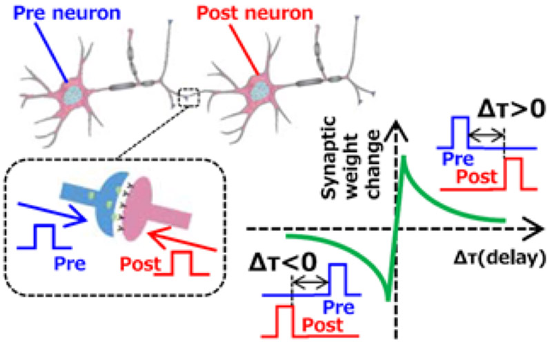
In order to realize spiking neural networks as hardware, devices that can reproduce neuronal functions are necessary. In this study, we fabricated a nonvolatile tunnel FET memory that can operate at both large memory capacity and low operation voltage, and showed that it can reproduce spike timing-dependent plasticity, one of the neuronal functions.
| Used equipment | EB lithography system, ion implantation, ICP-RIE #1, JEOL-SEM, thermal oxidation furnace, hydrogen annealing furnace, LP-CVD, plasma SiN-CVD, RTA #1, dual frequency excitation RIE, etc. |
|---|---|
| Article | H. Kino, T. Fukushima, and T. Tanaka, “Generation of STDP With Non-Volatile Tunnel-FET Memory for Large-Scale and Low-Power Spiking Neural Networks,” IEEE J. Electron Devices Soc., vol. 8, no. July, pp. 1266–1271, Mar. 2020, https://doi.org/10.1109/JEDS.2020.3025336 |
Compact spectrometers with plasmonic color filters
“Plasmonic color filters” that use metal nanostructures have various advantages over conventional color filters that use pigment absorption, such as the ability to collectively form filters with various color characteristics with a thickness of only a few tens of nanometers. By manufacturing plasmonic color filters on a photodiode array, we have developed a compact spectrometer that is miniaturized compared to conventional spectrometers and is small enough to fit on a fingertip.
| Used equipment | Laser lithography system, EB lithography system, mask aligner (SUSS), ion implantation, RTA, TEOS CVD, RF magnetron sputter, EB deposition, FAB, high resolution SEM |
|---|---|
| Article | Y. Kanamori, D. Ema, and K. Hane, “Miniature spectroscopes with two-dimensional guided-mode resonant metal grating filters integrated on a photodiode array,” Materials 11, 1924 (2018). https://doi.org/10.3390/ma11101924 |
Highly sensitive thermometer using a vacuum-packed Si resonator in a microfluidic chip for the thermal measurement of single cells
A silicon micromechanical resonator as a resonant temperature sensor and microchannel were fabricated in a microfluidic chip, which can measure the temperature of small objects in solutions. The cavity around the resonator can be evacuated to vacuum without interfering with the liquid-filled microchannel.
| Used equipment | Mask aligner (SUSS), ICP-RIE #2, microsystem analyzer |
|---|---|
| Article | Naoki Inomata, Masaya Toda, and Takahito Ono, “Highly sensitive thermometer using a vacuum-packed Si resonator in a microfluidic chip for the thermal measurement of single cells,” Lab on a Chip 16, 3597–3603 (2016). https://doi.org/10.1039/C6LC00949B |
Optical switch using MEMS-driven silicon waveguide
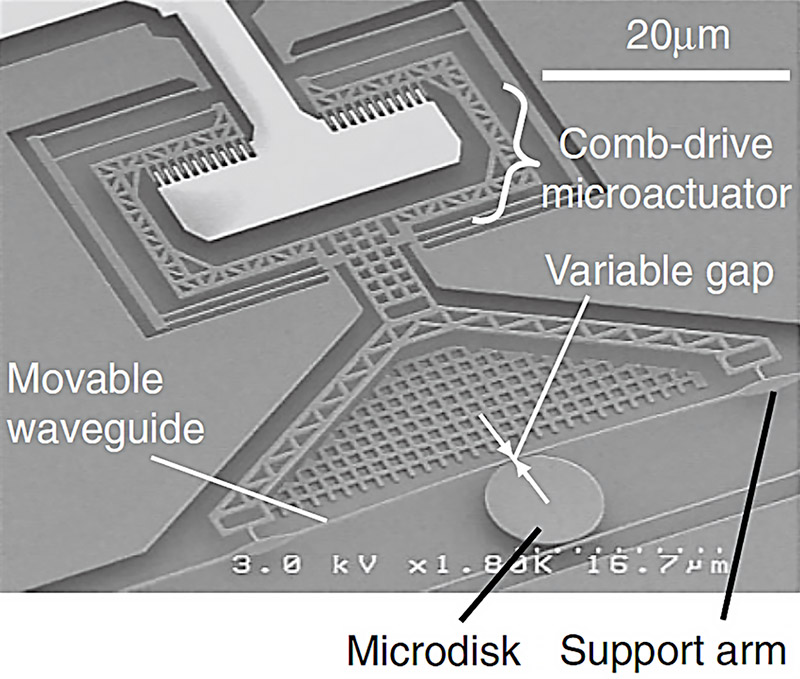
“Silicon waveguide” is an elemental technology of optical circuits that will play an important role for next-generation optical communication. We have developed an optical switch that switches the optical path by driving the silicon waveguide with a microactuator and controlling the optical coupling efficiency with the microdisk resonator.
| Used equipment | EB lithography system, FAB, high resolution SEM |
|---|---|
| Article | Y. Kanamori, Y. Sato, and K. Hane, “Fabrication of silicon microdisk resonators with movable waveguides for Control of Power Coupling Ratio,” Japanese Journal of Applied Physics 52, 06GL19 (2013). https://doi.org/10.7567/JJAP.52.06GL19 |
Three-dimensional-integrated STT-MRAM (spin transfer torque magnetic random-access memory)
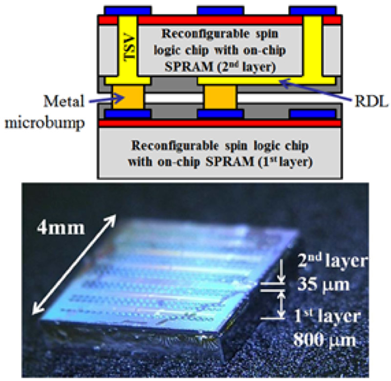
STT-MRAM is a magnetoresistive change memory that uses a data rewriting technique called spin transfer torque (STT), but it has the problem of low thermal endurance. In this study, we succeeded in three-dimensional integrated STT-MRAM using Through-Si Via (TSV) by suppressing the thermal load due to the integration process.
| Used equipment | Plasma/ozone TEOS CVD, EVG Bonder, JEOL-SEM, ICP-RIE #2 |
|---|---|
| Article | T. Tanaka, H. Kino, R. Nakazawa, K. Kiyoyama, H. Ohno, and M. Koyanagi, “Ultrafast parallel reconfiguration of 3D-stacked reconfigurable spin logic chip with on-chip SPRAM (SPin-transfer torque RAM),” in 2012 Symposium on VLSI Technology (VLSIT), Jun. 2012, pp. 169–170, https://doi.org/10.1109/VLSIT.2012.6242515 |
Reflectance-variable filters for optical communication using photonic crystals
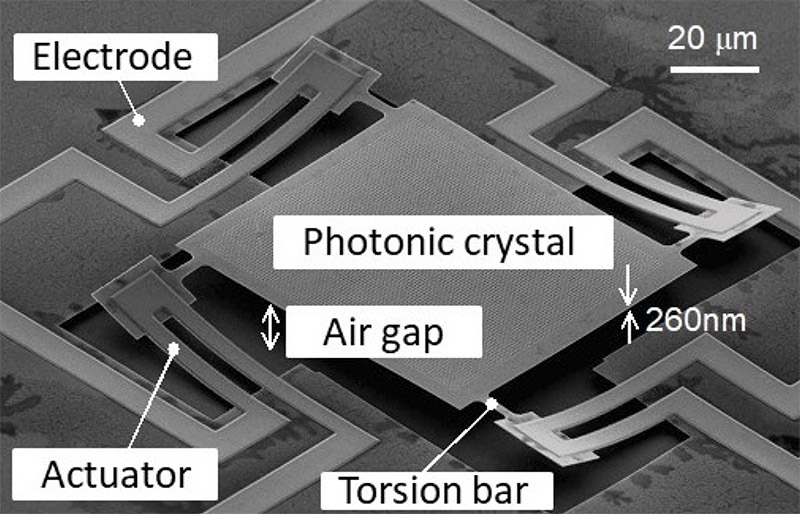
“Photonic crystal” is a fine periodic structure with the same size as the wavelength of light and has the function of blocking and confining light. We have developed a reflectance-variable filter that controls the optical coupling efficiency of a nano-optical resonator and controls the light blocking characteristics by controlling the position of the photonic crystal with high accuracy using a microactuator.
| Used equipment | EB lithography system, RF magnetron sputter (Shibaura), FAB, high resolution SEM |
|---|---|
| Article | Y. Kanamori, T. Kitani, and K. Hane, “Control of guided resonance in a photonic crystal slab using microelectromechanical actuators,” Applied Physics Letters 90, 031911 (2007). https://doi.org/10.1063/1.2431452 |