- table of contents
Surface treatment
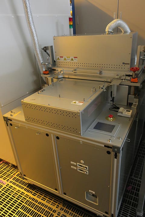
UV exposure
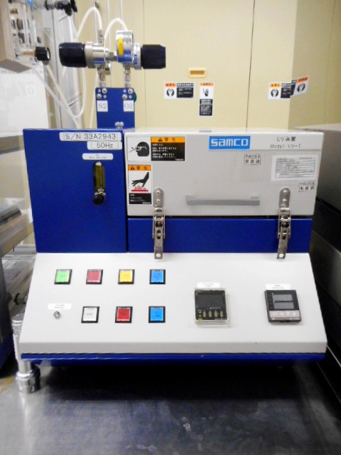
| Manufacturer name (model) | Samco (UV-T) |
|---|---|
| Use | Removal of organic substances by UV + O3, UV cure by UV + N2 |
| Main specifications | Light source: low pressure mercury lamp (253.7, 184.9 nm), Stage temperature setting range: Room temperature to 300 ℃ |
| Process gas | O3, O2, N2 |
| Sample size | Maximum ⌀200 mm, thickness 2 mm or less |
| Remarks |
Two-fluid cleaner
| Manufacturer name (model) | Actes (ADE-3000S) |
|---|---|
| Use | Two-fluid spray cleaning device using water or organic solvent (IPA, etc.) |
| Main specifications | Wafer rotation speed: 0 to 3000 rpm, wafer swing angle: 0 to 40° |
| Sample size | □20 mm or 4 inch |
| Remarks |
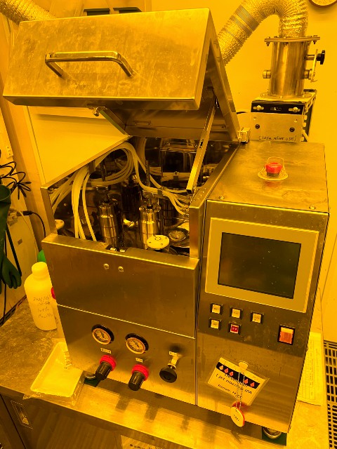
HDMS treatment system
| Manufacturer name (model) | Self-made |
|---|---|
| Use | Apply resist such as OFPR to the surface of the silicon wafer In some cases, surface treatment is more appropriate than OAP dripping. Since the series of treatments after washing with sulfuric acid hydrogen peroxide can be handled without touching the atmosphere, the possibility of resist coating failure is reduced. |
| Sample size | □20 mm–4 inch |
| Remarks |
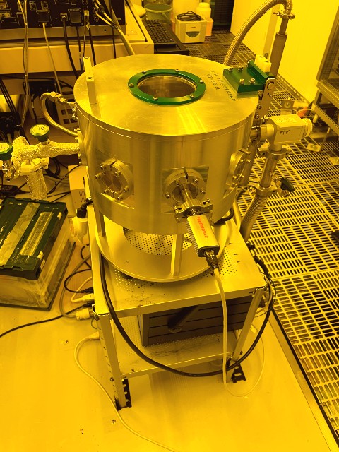
Supercritical CO2 drier
| Manufacturer name (model) | SC Fluids (CPD1100) |
|---|---|
| Application | Drying of MEMS device using supercritical |
| Sample size | Maximum 4 inch |
| Remarks |
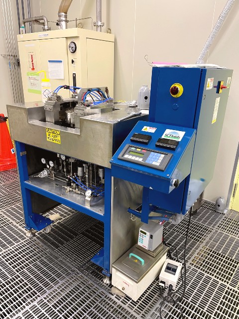
Excimer exposure
| Manufacturer name (model) | M. D. COM inc (MEIRA-M-1-330) |
|---|---|
| Application | Cleaning and decomposition of minute organic matter Hydrophilic modification and adhesion enhancement Obtaining nitride and oxide films Matt finish treatment for paint (curing) |
| Main specifications | Wavelength: 172nm, 1lamp, 50mW/cm² specification Stage moving irradiation system Nitrogen and/or CDA feeding possible Irradiation distance: 2 to 23mm |
| Sample size | Maximum 300mm square Substrate thickness up to 23mm can be treatment |
| Others | The sample transport stage enables uniform irradiation up to a maximum of 300 mm square |
| Remarks |