Size that can be placed on a square mesh of about 50 mm
Others
Example of film formation conditions: 600 V DC plasma, acetylene 10 Pa, hydrogen 100 Pa
Remarks
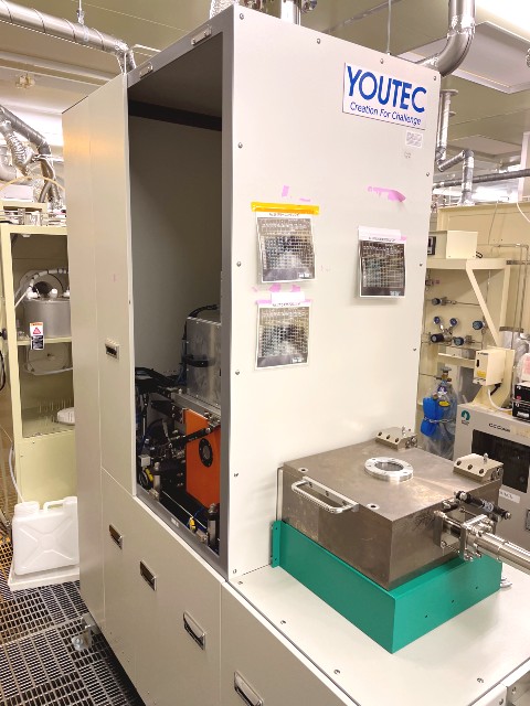
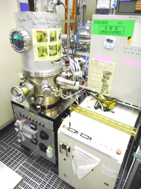
Plasma diamond CVD(AX3030)
Manufacturer name (model)
Seki Technotron (AX5200)
Type
MPECVD
Materials that can be deposited
Graphene nanowalls, diamond
Deposition temperature
RT–400 ℃
Deposition rate
Low
Sample size
10 × 10 mm
Others
Microwave power: 650 W , Gas: H2, CH4
Remarks
RF magnetron sputter(Shibaura#1,CFS-4ES)
Manufacturer name (model)
Shibaura Mechatronics (CFS-4ES)
Materials that can be deposited
Metallic and non-metal compatible
Samples that can be introduced
Durable and particle-free sample
Sample size
Maximum 4 inch × 2
Deposition temperature
RT–300 ℃
Process gas
Ar, O2, N2
Other
Maximum 300 W, 3 Target can be installed
Remarks
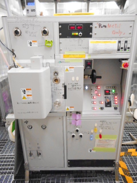
RF magnetron sputter(Shibaura#2,CFS-4ES)
Manufacturer name (model)
Shibaura Eletec (CFS-4ES-232)
Materials that can be formed
Pure metal only (other than magnetic material)
Samples that can be introduced
A sample that is resistant and does not generate particles
Sample size
Maximum 4 inch × 2
Deposition temperature
Room temperature
Process gas
Ar
Others
3 Targets can be installed
Remarks
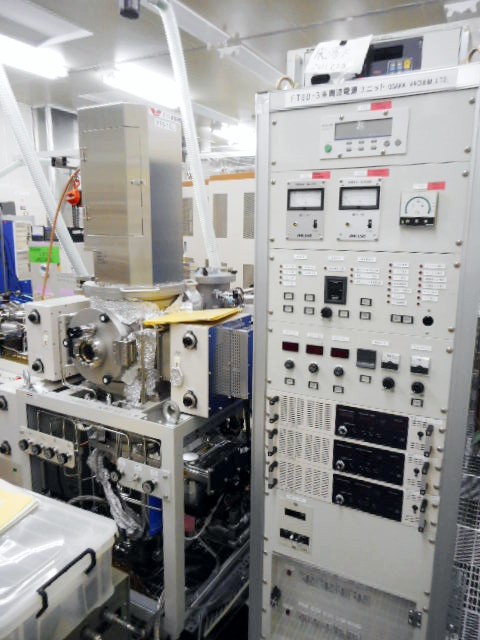
Facing target DC sputter
Manufacturer name (model)
Osaka Vacuum (FTS- R3S)
Materials that can form a film
Fe, Co, Ni
Samples that can be introduced
Samples that are sputter resistant and do not generate particles
Sample size
□20 mm× 4 sheets
Sample film formation temperature
RT–400 ℃
Process gas
Ar, Kr, N2
Other
Lift Can be turned off
Remarks
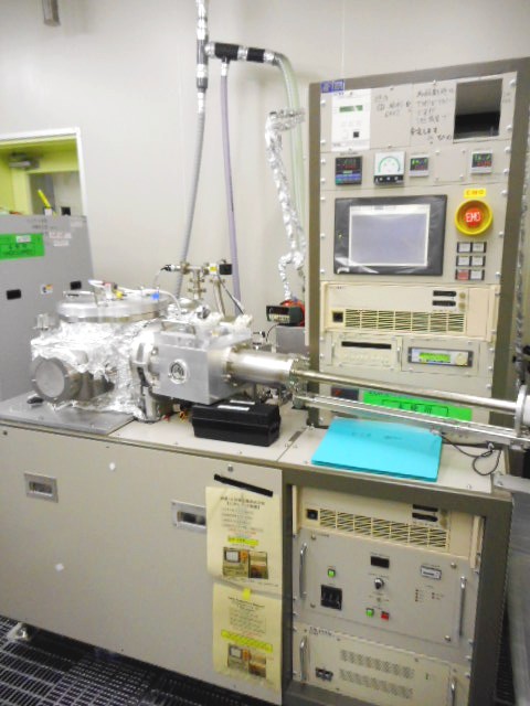
Facing target RF sputter
Manufacturer name (model)
Osaka Vacuum (FTS-1CL)(FTS-1CL)
Materials that can be deposited
Various metals
Sample size
□20 mm
Deposition temperature
RT–700 ° C
ProcessGas
Ar
Others
Organic material NG
Remarks
ECR Sputter
Manufacturer name (model)
JSW Afty (AFTEX EC-2300)
Materials that can be formed]
AlN only
Samples that can be introduced
Spatter resistant and particles that does not occur
Sample size
4 inch, □20 mm
Formation temperature
RT–300 ℃
Process gas
Ar + N2
Others
Lift-off not possible
Remarks
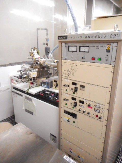
ECR ion beam sputter(EIS-220)
Manufacturer name (model)
Elionix (EIS-220)
Materials that can be deposited
Semiconductors, materials for MEMS, etc.
Sample size
Maximum 3 inch
Capsulation temperature
RT–350 ℃
Process gas
Ar, N2
Others
Organic matter OK, lift-off possible
Remarks
RF magnetron sputter(ANELVA#1,SPC-350)
Manufacturer name (model)
Anelva (SPC-350)
Materials that can be formed
Metal, Si, SiO2
Samples that can be introduced
Spatter resistant and generation of particles No sample
Sample size
Maximum ⌀2 inch
Deposition temperature
RT–400 ℃
Process gas
Ar, O2, N2
Others
Organic material NG, lift-off not possible, reactive sputtering possible, load lock chamber available, 3 Target can be installed
Remarks
High-temp RF magnetron sputter(SSP3000)
Manufacturer name (model)
Suga (SSP3000)
Materials that can be deposited
Metal
Sample size
Maximum 2 inch × 2
temperature
RT-600 ℃
Process gas
Ar, N2, O2
Remarks
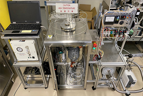
Thermal oxidation furnace
Manufacturer name (model)
Self-made
Materials that can be deposited
SiO2
Sample size
⌀2 inch
Applications (features)
Wet and dry oxidation of Si
Deposition temperature
About 1000 ℃
Main specifications
Gas type: O2, H2, N2
Others
Mainly for transistor gate insulating film and LOCOS process
Remarks
EB evaporation
Manufacturer name (model)
ANELVA (EGP-230)
Sample size
□20 mm, ⌀4 inch, etc.
Applications (features)
Film formation for lift-off, etc
Main specifications
Film formation is possible with a vacuum degree 10−6 Torr. Metal film and insulating film can be formed. Titanium and aluminum are shared, but other materials are raw materials and hearth liners are prepared by each person. Magnetic materials such as nickel cannot be deposited. The film thickness can be controlled by a crystal oscillation type film thickness meter.
Others
Operation between users is prohibited for manual devices. Since the absorber inside the cryopump has a limited life, continuous operation is prohibited all night.
Remarks
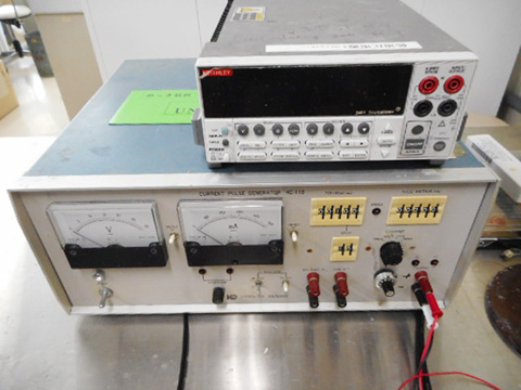
Electroplating #1(2401)
Manufacturer name (model)
KEITHLEY (2401 DC current)
Sample size
Depends on the beaker, solution tank size, and amount of plating solution to bring. 20 × 20 mm is standard for the range of accessories.
Application (feature)
Plating mainly by direct current control.
Others
Prepare the plating solution by yourself.
Remarks
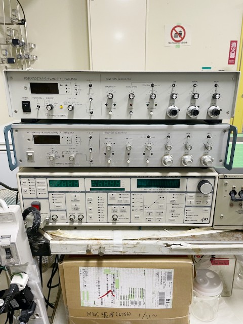
Electroplating #2(HAB-151A)
Manufacturer name (model)
Hokuto Denko (HAB-151 Potential Shot)
Sample size
Depends on the beaker, solution tank size, and amount of plating solution to bring. 20 × 20 mm is standard for the range of accessories.
Applications (features)
Mainly for measurement of redox potential and three-electrode plating. A device for conducting electrochemical experiments by controlling the electric potential.
Others
Prepare the plating solution by yourself. There is an accessory device for conducting experiments on nitrogen gas atmosphere.
Remarks
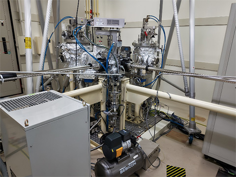
MBE
Manufacturer name (model)
Riber (Riber MBE 32 system)
Type
MBE
Materials that can be deposited
GaN, AlN, InN
Film film temperature
900 ℃
Film film rate
100 nm/h
Sample size
⌀3 inch
Others
Remarks
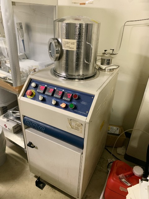
Palylene evaporator
Manufacturer name (model)
Specialty Coating System (PDS2010)
Sample size
Maximum 120 × 120 mm
Use
Parylene
Main specifications
Film formation pressure: approximately 3 Pa
Deposition temperature:RT
film formation rate: 3 μm/h
Remarks
PLD
Manufacturer name (model)
Pascal
Sample size
□20 mm
Use (features)
Deposit of oxide thin film
Remarks
ALD
Manufacturer name (model)
Cambridge NanoTech (Savannah S100)
Type
Thermal ALD (Atomic Layer Deposition)
Materials that can be deposited
Al2O3 (TMA + H2O)
Deposition Temperature
100℃–220℃
Deposition rate
0.11 nm/cycle
Sample size
Maximum ⌀4 inch
Others
Remarks
RF magnetron sputter(ANELVA#2,SPC-350UHV)
Manufacturer name (model)
Anelva (SPH-350)
Materials that can be formed
AlN, ScAlN
Samples that can be introduced
Si, Glass, etc. (photoresist or polymers is NG)
Sample size
2cm□
Deposition temperature
200°C
Process gas
Ar, N2
Others
Remarks
Loading several samples at one time is possible
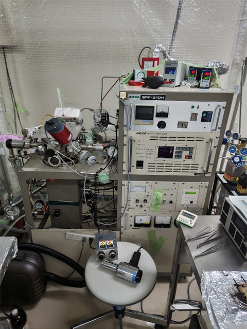
Sputter machine for Pb based complex oxide(SPF-210H)
Manufacturer name (model)
ANELVA (SPF-210H)
Type
RF magnetron sputtering
Sample size
Maximum 2 cm□
Materials that can form a film
PZT, PMN-PT
Sample film formation temperature
Maximum 600 ℃
Deposition rate
400–550 nm/h
Process gas
Ar, O2
Remarks
To use the equipment, you need to consult with the equipment manager of the Shuji Tanaka Laboratory.