Others (plasma excitation method, power supply output, etc.)
Plasma excitation method: CCP
Remarks
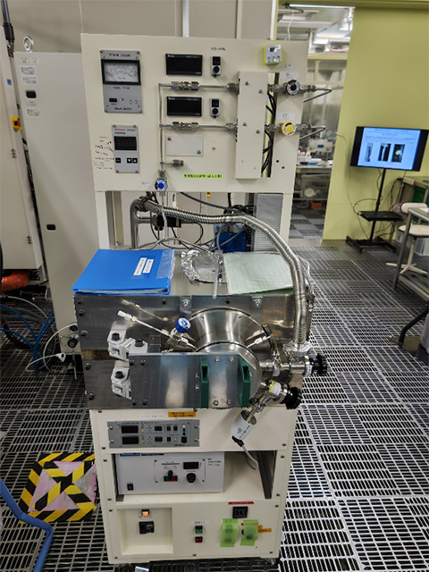
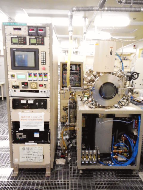
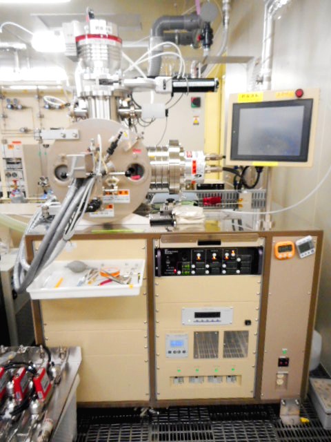
Ion beam milling
Manufacturer name (model)
Hakuto Co., Ltd. (IBE-KDC 75)
Application
Microfabrication of materials (Pt, etc.) that cannot be handled by RIE equipment
Microfabrication of materials (Pt, etc.) that cannot be handled by RIE equipment
Ar
Sample size
20 mm, 3 inch, 4 inch
Materials that can be introduced
Other than harmful substances (Pb, As, etc.), other than low vapor pressure substances (Zn, etc.)
Etching rate
Pt 30 nm/min
Others (plasma excitation method, power supply output, etc.)
Kaufman type plasma generator
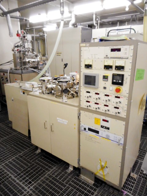
Remarks
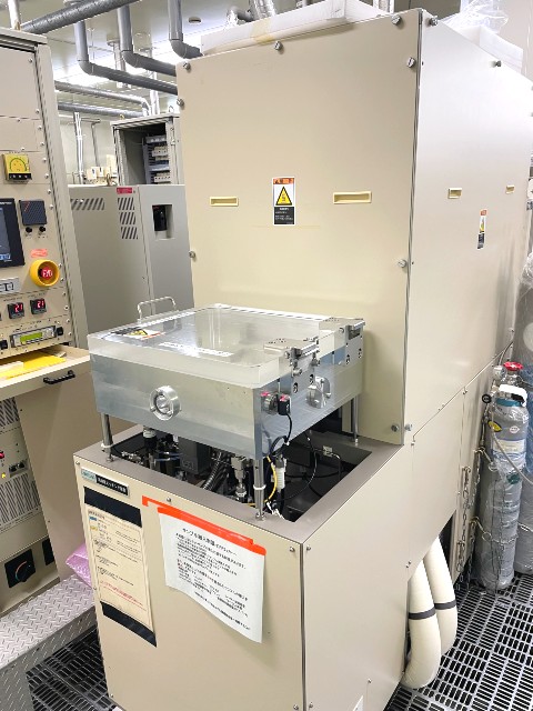
Dual frequency RIE
Manufacturer name (model)
ANELVA (L-211D)
Use
For source / drain contact etching
Process gas
C4F8, Ar, O2
SampleSize
⌀2 inch
Workable material
Si substrate
Etching rate
300 nm/min
Selection ratio
1:10
Others (plasma excitation method, power supply output, etc.)
Dual frequency excitation
Remarks
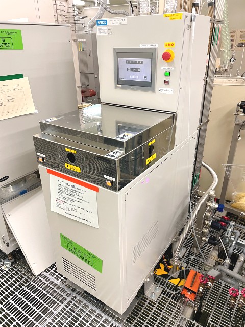
SiN etcher
Manufacturer name (Manufacturer name) Model)
Samco (RIE-10NR)
Use
For SiN etching of LOCOS
Process gas
CF4, H2, O2, SF6
Sample size
⌀2 inch
Workable material
Si substrate
Etching rate
100 nm/min
Selection ratio
1:10
Others (plasma excitation method, power supply output, etc.)
Parallel plate type
Remarks
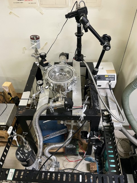
Isotropic Si etcher
Manufacturer name (model)
Self-made
Applications
Si selective etching
Process gas
XeF2
Workable materials
Si, SiO2, positive resist, metal
Sample size
□20 mm
Etching rate
Varies depending on the area of the material to be processed
Selection ratio
10000 (SiO2)
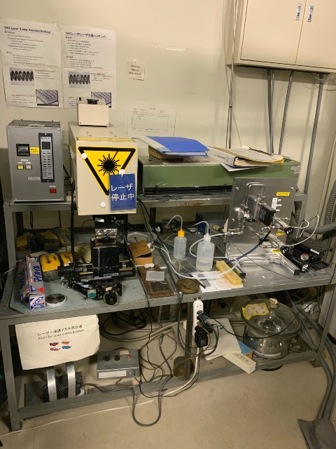
Remarks
YAG laser
Manufacturer name (model)
NEC (Nd:YAG Laser SL 115G)
Features/Applications
Dry Process & local processing, separation of manufactured devices, cutting of stainless steel, SMA, etc. and selective removal of coatings on welded metal wires, PZT laser-assisted etching