Bond alignment is possible with the EVG mask aligner installed in this facility
Remarks
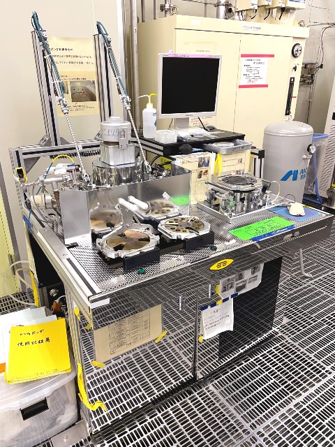
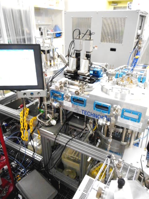
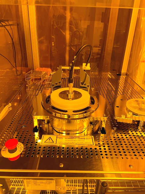
Wafer bonder (Technofine)
Manufacturer name (model)
Technofine (SG-560)
Maximum sample size
4 inch
Maximum generated force (load)
10000 N
Maximum temperature
350 ℃
Chamber vacuum
5 x 10⁻³ Pa
Maximum applied voltage
Not compatible
Remarks
Flip chip bonder #1
Manufacturer name (model)
Kan Electronics (MODEL6000)
Maximum sample size
□20 mm
Maximum generated force (load)
5 kgf (49 N)
Maximum temperature
200 ℃
Chamber vacuum degree
Atmospheric pressure (N2 gas flow possible)
Maximum applied voltage
No voltage applied
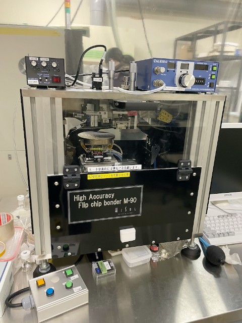
Remarks
Flip chip bonder#2(M-90-10)
Manufacturer name (model)
HiSOL (M-90)
Maximum sample size
Top: □10 mm, bottom (Stage): 4 inch
Maximum generated force (load)
5.5 N
Maximum temperature
350 ℃
Chamber vacuum
Atmospheric pressure
Maximum applied voltage
Voltage cannot be applied
Remarks
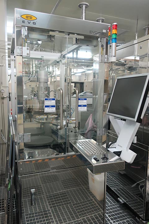
EVG plasma activator
Manufacturer name (manufacturer name) Model)
EV Group (EVG810)
Maximum sample size
6 inch
Chamber vacuum
About 1 Pa
Others
Applications for sample surface plasma treatment for low-temperature direct bonding
Remarks
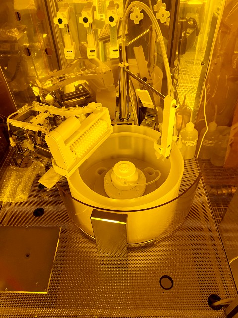
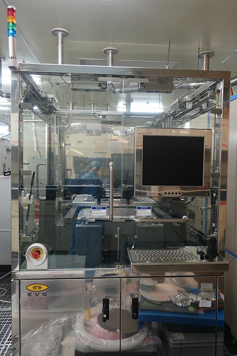
Megasonic Cleaner
Manufacturer name (model)
EV Group (EVG301)
Maximum sample size
6 inch
Others
Applications for megasonic cleaning of the sample surface before treatment with the EVG plasma surface activation device, sample cleaning with a brush is possible